- 您现在的位置:买卖IC网 > Sheet目录491 > NTMS4917NR2G (ON Semiconductor)MOSFET N-CH 30V 10.2A SO8 FL
NTMS4917N
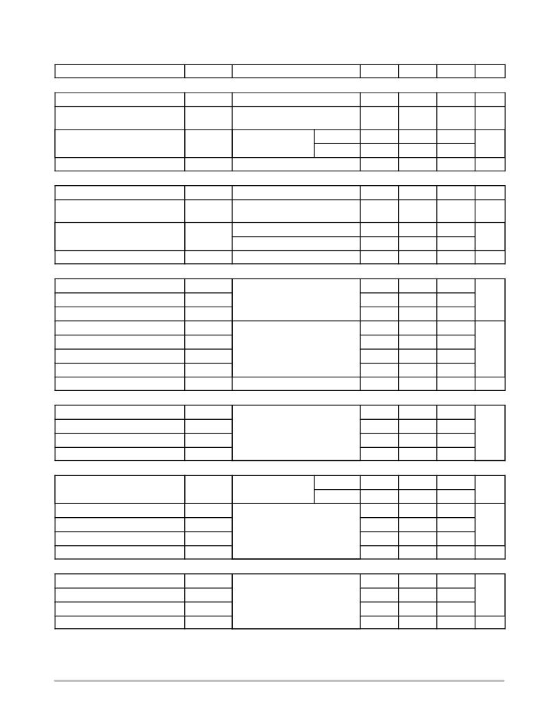
ELECTRICAL CHARACTERISTICS (T J = 25 ° C unless otherwise specified)
Parameter
Symbol
Test Condition
Min
Typ
Max
Unit
OFF CHARACTERISTICS
Drain ? to ? Source Breakdown Voltage
Drain ? to ? Source Breakdown Voltage
Temperature Coefficient
V (BR)DSS
V (BR)DSS /T J
V GS = 0 V, I D = 250 m A
30
16
V
mV/ ° C
Zero Gate Voltage Drain Current
I DSS
V GS = 0 V, V DS = 30 V
T J = 25 ° C
T J = 125 ° C
1.0
10
m A
Gate ? to ? Source Leakage Current
I GSS
V DS = 0 V, V GS = ± 20 V
± 100
nA
ON CHARACTERISTICS (Note 3)
Gate Threshold Voltage
V GS(TH)
V GS = V DS , I D = 250 m A
1.0
1.7
2.5
V
Negative Threshold Temperature
Coefficient
V GS(TH) /T J
5
mV/ ° C
Drain ? to ? Source On Resistance
R DS(on)
V GS = 10 V, I D = 11 A
8.25
11
m W
V GS = 4.5 V, I D = 9 A
11.25
15
Forward Transconductance
g FS
V DS = 1.5 V, I D = 7.5 A
19
S
CHARGES, CAPACITANCES AND GATE RESISTANCE
Input Capacitance
C iss
1054
pF
Output Capacitance
Reverse Transfer Capacitance
C oss
C rss
V GS = 0 V, f = 1.0 MHz, V DS = 25 V
325
165
Total Gate Charge
Q G(TOT)
15.6
nC
Threshold Gate Charge
Gate ? to ? Source Charge
Gate ? to ? Drain Charge
Q G(TH)
Q GS
Q GD
V GS = 4.5 V, V DS = 15 V, I D = 7.5 A
2.6
4.2
7
Total Gate Charge
Q G(TOT)
V GS = 10 V, V DS = 15 V, I D = 7.5 A
29
nC
SWITCHING CHARACTERISTICS (Note 4)
Turn ? On Delay Time
t d(on)
8.5
ns
Rise Time
Turn ? Off Delay Time
Fall Time
t r
t d(off)
t f
V GS = 10 V, V DS = 15 V,
I D = 1.0 A, R G = 6.0 W
6.3
27
12
DRAIN ? SOURCE DIODE CHARACTERISTICS
Forward Diode Voltage
V SD
V GS = 0 V, I S = 2.0 A
T J = 25 ° C
T J = 125 ° C
0.75
0.58
1.0
V
Reverse Recovery Time
t RR
28
ns
Charge Time
Discharge Time
t a
t b
V GS = 0 V, d IS /d t = 100 A/ m s,
I S = 2.0 A
12.2
15.7
Reverse Recovery Charge
Q RR
20
nC
PACKAGE PARASITIC VALUES
Source Inductance
L S
0.66
nH
Drain Inductance
Gate Inductance
L D
L G
T A = 25 ° C
0.2
1.5
Gate Resistance
R G
0.70
W
3. Pulse Test: pulse width = 300 m s, duty cycle v 2%.
4. Switching characteristics are independent of operating junction temperatures.
http://onsemi.com
2
发布紧急采购,3分钟左右您将得到回复。
相关PDF资料
NTMS4920NR2G
MOSFET N-CH 30V 10.6A 8SOIC
NTMS4935NR2G
MOSFET N-CH 30V 10A 8SOIC
NTMS4937NR2G
MOSFET N-CH 30V 8.6A 8SOIC
NTMS4N01R2G
MOSFET N-CH 20V 3.3A 8-SOIC
NTMS5835NLR2G
MOSFET N-CH 40V 9.2A 8SOIC
NTMS5838NLR2G
MOSFET N-CH 40V 7.5A 8SOIC
NTMS5P02R2SG
MOSFET P-CH 20V 3.95A 8SOIC
NTMS7N03R2
MOSFET N-CH 30V 4.8A 8-SOIC
相关代理商/技术参数
NTMS4920N
制造商:ONSEMI 制造商全称:ON Semiconductor 功能描述:Power MOSFET 30 V, 17 A, N−Channel, SO−8
NTMS4920NR2G
功能描述:MOSFET 30V 136A 4.3 mOhm Single N-Chan SO-8 RoHS:否 制造商:STMicroelectronics 晶体管极性:N-Channel 汲极/源极击穿电压:650 V 闸/源击穿电压:25 V 漏极连续电流:130 A 电阻汲极/源极 RDS(导通):0.014 Ohms 配置:Single 最大工作温度: 安装风格:Through Hole 封装 / 箱体:Max247 封装:Tube
NTMS4935N
制造商:ONSEMI 制造商全称:ON Semiconductor 功能描述:Power MOSFET 30 V, 16 A, N−Channel, SO−8
NTMS4935NR2G
功能描述:MOSFET Power MOSFET 30V 126A 5.1 mOhm Single RoHS:否 制造商:STMicroelectronics 晶体管极性:N-Channel 汲极/源极击穿电压:650 V 闸/源击穿电压:25 V 漏极连续电流:130 A 电阻汲极/源极 RDS(导通):0.014 Ohms 配置:Single 最大工作温度: 安装风格:Through Hole 封装 / 箱体:Max247 封装:Tube
NTMS4937N
制造商:ONSEMI 制造商全称:ON Semiconductor 功能描述:Power MOSFET Power MOSFET
NTMS4937NR2G
功能描述:MOSFET Power MOSFET 30V 112A 6.5 mOhm Single RoHS:否 制造商:STMicroelectronics 晶体管极性:N-Channel 汲极/源极击穿电压:650 V 闸/源击穿电压:25 V 漏极连续电流:130 A 电阻汲极/源极 RDS(导通):0.014 Ohms 配置:Single 最大工作温度: 安装风格:Through Hole 封装 / 箱体:Max247 封装:Tube
NTMS4939N
制造商:ONSEMI 制造商全称:ON Semiconductor 功能描述:Power MOSFET 30 V, 12.5 A, N−Channel, SO−8
NTMS4939NR2G
功能描述:MOSFET Power MOSFET 30V 100A 8.4 mOhm Single RoHS:否 制造商:STMicroelectronics 晶体管极性:N-Channel 汲极/源极击穿电压:650 V 闸/源击穿电压:25 V 漏极连续电流:130 A 电阻汲极/源极 RDS(导通):0.014 Ohms 配置:Single 最大工作温度: 安装风格:Through Hole 封装 / 箱体:Max247 封装:Tube
